LITTLE FS https://github.com/littlefs-project/littlefs
https://github.com/lurk101/pico-littlefs
https://github.com/oyama/pico-vfs
http://frstcomputer.com/ Jon at Hope / GTLUG / ALE ( Gopherhole: jonsharp.net )
(From Cloud9's website): Here's a simple test that will determine if your Mulit-Pak has already been upgraded to work with a CoCo 3. From BASIC's OK prompt, type PRINT PEEK(&HFF90) and press ENTER. If 126 is returned then the Multi-Pak has been upgraded. If it returns 255 then it has NOT been upgraded.
https://www.aliexpress.us/item/3256805082503789.html 1.44寸èµæï¼
æä¾å ¨å¥èµæï¼http://pan.baidu.com/s/1gd49RMV
1ãLCD size: 1.44 inches
2ãDot matrix size: 240*240 can be adjusted to show the reverse, horizontal and vertical screen can be
3ãLCD colour: 65K full colour
4ãHardware interface: SPI interface
5ãDriver IC: ST7896
6ãOperating temperature: -20-70
7ãWorking power:3.3v
8ãInterface:8Pin
1ãGND:Power ground
2.VCC:3.3v-5.0v DC
3.SCL:SPI clock line
4. SDA:SPI data line
5. RES:Restart interface
6. DC:SPI data/command selection
7,Cs:Chip select interface/1.3" no
8,BLK: Backlight control, default floating, low OD3 level off
https://github.com/LifeWithDavid/Raspberry-Pi-Pico-PIO/blob/fc3e25c3d254869be01189d5546fb8b737f302c3/Episode%2012%20Files.txt (Life With David)
https://stackoverflow.com/questions/76540246/raspberry-pi-pico-64-color-vga
https://github.com/silvervest/c64pico ( Commodore 64 on Pico ) https://github.com/bobricius/PICOmputer
https://www.raspberrypi.com/news/commodore-64-raspberry-pi-pico-emulator/
https://github.com/raspberrypi/pico-playground ( has VGA schematic; scroll down )
https://shop.pimoroni.com/products/pimoroni-pico-vga-demo-base?variant=32369520672851
https://github.com/kilograham/rp2040-doom/releases
https://anycpu.org/forum/viewtopic.php?f=23&t=978 "DIP-8: 8-bit TTL computer"
https://github.com/jimjag/JJ65c02
http://axio.ms//projects/2024/06/16/MicroMac.html
https://www.google.com/search?q=NEO6502
https://retrogamecoders.com/neo6502-review/
https://retrogamecoders.com/wp-content/uploads/2024/02/Screenshot-by-Dropbox-Capture-2.png
https://github.com/OLIMEX/Neo6502/blob/main/HARDWARE/Neo6502-rev-B1/Neo6502_Rev_B1.pdf
https://www.makerhacks.com/z80-io-lcd/
https://damieng.com/typography/zx-origins/
https://hackaday.com/2023/08/07/all-about-usb-c-example-circuits/
https://www.digikey.com/en/products/detail/adafruit-industries-llc/1833/5629431?
https://github.com/JayesonLS/TandyCircuitsAndLogic/tree/master
74LVC245A-Q100;
74LVCH245A-Q100
Octal bus transceiver; 3-state
The 74LVC245A-Q100; 74LVCH245A-Q100 is an 8-bit transceiver with 3-state outputs. The device features an output enable (OE) and send/receive (DIR) for direction control. A HIGH on OE causes the outputs to assume a high-impedance OFF-state. Inputs can be driven from either 3.3 V or 5 V devices. This feature allows the use of these devices as translators in mixed 3.3 V and 5 V environments.
74LVC273
Octal D-type flip-flop with reset; positive-edge trigger
The 74LVC273 is an octal positive-edge triggered D-type flip-flop. The device features clock (CP) and master reset (MR) inputs. The outputs Qn will assume the state of their corresponding D inputs that meet the set-up and hold time requirements on the LOW-to-HIGH clock (CP) transition. A LOW on MR forces the outputs LOW independently of clock and data inputs. Inputs can be driven from either 3.3 V or 5 V devices. This feature allows the use of these devices as translators in mixed 3.3 V and 5 V environments.
74LVC374A
Octal D-type flip-flop; 5 V tolerant inputs/outputs;
positive-edge trigger; 3-state
The 74LVC374A is an octal positive-edge triggered D-type flip-flop with 3-state outputs. The device features a clock (CP) and output enable (OE) inputs. The flip-flops will store the state of their individual D-inputs that meet the set-up and hold time requirements on the LOW-to-HIGH clock (CP) transition. A HIGH on OE causes the outputs to assume a high-impedance OFF-state. Operation of the OE input does not affect the state of the flip-flops. Inputs can be driven from either 3.3 V or 5 V devices. This feature allows the use of these devices as translators in mixed 3.3 V and 5 V environments.
74LVC138A
3-to-8 line decoder/demultiplexer; inverting
The 74LVC138A decodes three binary weighted address inputs (A0, A1 and A2) to eight mutually exclusive outputs (Y0 to Y7). The 74LVC138A features three enable inputs (E1, E2 and E3). Every output will be HIGH unless E1 and E2 are LOW and E3 is HIGH. This multiple enable function allows easy parallel expansion of the 74LVC138A to a 1-of-32 (5 to 32 lines) decoder with just four 74LVC138A ICs and one inverter. The 74LVC138A can be used as an eight output demultiplexer by using one of the active LOW enable inputs as the data input and the remaining enable inputs as strobes. Inputs can be driven from either 3.3 V or 5 V devices. This feature allows the use of these devices as translators in mixed 3.3 V and 5 V environments.
74LVC4066-Q100
Quad bilateral switch
The 74LVC4066-Q100 is a high-speed Si-gate CMOS device.
The 74LVC4066-Q100 provides four single pole, single-throw analog switch functions. Each switch has two input/output terminals (nY and nZ) and an active HIGH enable input (nE). When nE is LOW, the analog switch is turned off.
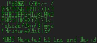
Constructed from https://github.com/dmadole/Nametag :

TINY CHEAP LCDs
HiLetgo HiLetgo 2pcs 1.3" IIC I2C Serial 128x64 SSH1106 OLED LCD Display LCD Module for Arduino AVR PIC STM32 https://www.amazon.com/gp/product/B07BHHV844/ref=ox_sc_act_title_3 http://www.hiletgo.com/ProductDetail/2157359.html
To drive an SSH1106-based OLED display with an Arduino, you will need a compatible library. The SSH1106 driver chip is similar to the more common SSD1306, but there are some key differences, particularly in how the display memory is handled (SSH1106 has a 132x64 memory, while SSD1306 has 128x64). Here's how you can find and use an SSH1106 driver for Arduino: 1. Using the Arduino Library Manager: Open the Arduino IDE. Go to Sketch > Include Library > Manage Libraries... In the Library Manager, search for "SH1106". You will likely find several options, including libraries based on the Adafruit GFX library, which is a popular choice for graphics on embedded displays. Look for libraries specifically mentioning SH1106 support. Install the desired library. 2. Manual Installation from GitHub: If you find a specific SH1106 library on GitHub (e.g., rene-mt/esp8266-oled-sh1106 or fcgdam/Adafruit_SH1106 for STM32 compatibility), you can download it as a ZIP file. In the Arduino IDE, go to Sketch > Include Library > Add .ZIP Library... and select the downloaded ZIP file. 3. Example Usage: Once the library is installed, you can use example code provided with the library or adapt existing SSD1306 examples. Key differences will be in the initialization of the display object and potentially in how the display() function is called. Example (using an Adafruit-compatible SH1106 library): C++ #include <Adafruit_SH1106.h> #include <Adafruit_GFX.h> // Required for graphics functions #define OLED_RESET 4 // Or the pin you're using for reset, if any Adafruit_SH1106 display(OLED_RESET); // Initialize with reset pin void setup() { Serial.begin(9600); // Initialize with I2C address (common addresses are 0x3C or 0x3D) // SH1106_SWITCHCAPVCC is a common power mode display.begin(SH1106_SWITCHCAPVCC, 0x3C); // Clear the buffer display.clearDisplay(); // Display text display.setTextSize(1); display.setTextColor(WHITE); display.setCursor(0,0); display.println("Hello, SH1106!"); display.display(); // Show the buffer content on the screen } void loop() { // Your main code here }Important Notes: I2C Address: Ensure you use the correct I2C address for your specific SSH1106 OLED module (commonly 0x3C or 0x3D). Reset Pin: Some modules may not require a dedicated reset pin, in which case you can adjust the constructor or use a dummy pin. Compatibility: While some libraries aim for compatibility with Adafruit's GFX library, always refer to the specific library's documentation for detailed instructions and function calls.
https://github.com/winneymj/SH1106
https://github.com/daschr/pico-ssd1306
Thermometer
https://github.com/jondurrant/RP2040PIO-DS18B20
https://github.com/adamboardman/pico-onewire
https://github.com/tjko/pico-1wire-lib
( linked from this fake bug: https://forums.raspberrypi.com/viewtopic.php?t=386626 )
PIR Motion Sensor
https://learn.adafruit.com/pir-passive-infrared-proximity-motion-sensor/overview